- Electrical Housing Box:
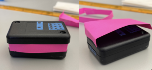
The housing electrical housing box will hold all of the electronic components to log data while the participant is wearing the device. One main goal for the housing unit is for the unit to be as small as possible so it does not impede on the participant’s day-to-day activity. Initial electrical housing models were created using cardstock paper and tape, measuring roughly 9 x 5 x 2 cm. We based the size on current device’s size, and it served as a baseline for our box size expectations. Then, each paper model was equipped with a different method of attaching to the body. One had a belt clip, one had a cross body design, and the last had a combination of both. Figure 11 shows the cross-body prototype and the all-in-one version as a necklace. These models allowed us to gather initial data on preferences for how to wear the device on the designs in an inexpensive and rapid way.

Figure 11. Paper Prototypes, cross-body (left), all in one – worn as necklace (right)
- Custom Box Designs:
Model I:
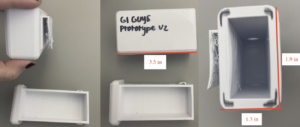
Next, a housing model was created on Autodesk Inventor based on the feedback we receive, about size of the device and how the device can be worn from the initial paper models, see Initial Feasibility Tests and Preliminary Results. The design featured an insert with a shell so the electrical components could easily be accessed. A locking system was created with tabs that could be pushed in to release the inside sliding part. The design included a belt clip for attaching to clothes or a belt. The model was printed using PLA filament. The printer does not print with supports, so some elements of the print became warped during printing, as seen in Figure 12.

Figure 12. First prototype of electrical housing box
Model II:
The next iteration of the prototype included updates to the Inventor file. The walls of the shell were thinned by approximately half its original thickness and modifications were made to the sides to allow for the locking system to work. The belt clip was adjusted to increase malleability. The model was printed in ABS plastic with dissolvable supports. Figure 13 shows version 3 of the prototype. This allowed for a cleaner print with stronger material, but it also made the housing unit heavier. This led us to make more modifications to the design to reduce weight and improve ease of use.

Figure 13. Prototype 3 of electrical housing unit. Printed in ABS with support material
Model III:
The next iteration of the printed box design included ventilation holes and cut outs in the walls to decrease the weight. These edits can be seen in Figure 14. The ventilation holes are along the sides of the box and the sliding insert, and roughly align, so air will flow over the electronics to help keep them from overheating. Holes were added for ventilation to assist with cooling the MCU and battery. The holes for the locking system are tapered to make it easier to push the locking buttons. This design includes a smaller belt clip with a split. The smaller footprint for the belt clip is to help the box feel less bulky while being worn. We have not decided upon if a slit will be helpful in the belt clip to add more flexibility to the plastic. While it could add flexibility it could also make the belt clip weaker and more prone to breaking. So, if we decide to go forward with the custom design this will have to be something we experiment with.

Figure 14. Updated inventor file for box shell (right) and insert (left).
- Modified Commercial Box Design:
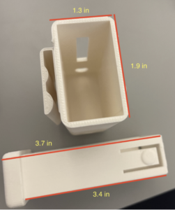
Another method of prototyping included a premade electrical housing from Poly Case, shown in Figure 15. The KT-35 and KT-45 units were purchased and then, metal belt clips from Amazon were attached. The boxes with the belt clips can be seen in Figure 16. These boxes were also smaller than the printed models, which allowed us to see if our electrical components would fit into a smaller box and if we would be able to make these sizes work for our device.

Figure 15. Dimensions of the Poly Case Boxes

Figure 16. Poly Case Boxes with belt clips attached with duct tape
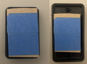
The Poly Case boxes required us to add our own holes for ventilation and wiring, and to attach the belt clip. Therefore, it is necessary to experiment where the holes must go on each box to prevent weakening the structural integrity of the box. We marked the necessary holes with painter’s tape and put them on the box to visualize the different types of holes, as seen in Figure 17 and 18.
One step that went through a few iterations was the shape of the ventilation holes. In the Figures, one can see that there are different shapes for the hole like lines, circles, and waves. The purpose of the ventilation holes is to allow air to pass through to cool the MCU if it gets hot. The shape of the hole only had aesthetic purposes, but the shape could leave the box weaker and more prone to breaking. Going forward we will use the round holes, when doing testing, such as compression testing, they are the easiest holes to create in the box design using a drill.

Figure 17. Markings for where holes could go (front of box)

Figure 18. Markings for where holes could go (back of box)
One consideration with the commercial boxes is that the size of them is predetermined. This lack of customization means that we must ensure that all of the electronic components must fit into the box to use it. To test this, we created models out of wood and cardboard to reflect the size of different electrical components and ensure that they could all fit into the box. From our testing we determined that all of the components could fit into the smallest box. Figure 19 shows the potential layouts we looked at for the seeed and Teensy boards. The Teensy 4.1 board just fits into the KT-35, which is the smaller of the two poly case boxes. Doing this test demonstrates that the electronic components will fit into the box.

Figure 19. Cardboard and wood cutouts to play with layout possibilities in poly case box KT-35
Another consideration would be the battery and how that would fit into the box, with the custom boxes room can be made for the battery to fit, but when thinking about the commercial boxes, the battery may not fit with enough room to allow for expansion, see Figure 20. The cardboard cutout is roughly the size of the current LiPo battery used to power the device, as we are still exploring if smaller batteries can be used. This meant that we needed to begin to consider options for attaching the battery on the outside of the box. One option was to print a holder that would mount onto the outside of the poly case box, and other option was to print out an expander that would mount on the inside of the box, paper prototypes of these ideas can be seen in Figure 21.

Figure 20. Cardboard model of the lithium battery currently used for device in the poly case boxes KT-35 (left) and KT-45 (right)

Figure 21. Paper models of solutions to attach battery to Poly Case KT-35 box
After looking at various ways to create our housing unit, Table 1 shows the pros and cons we found for each type of device. Each has different benefits and depending on the final layout of the circuit board. Ultimately our hope is to finalize our housing unit early in the winter term.
| Prototype: | Pros: | Cons: |
| PLA Printed Box |
|
|
| ABS Printed Box |
|
|
| Poly Case Boxes |
|
|
Table 1: Pros and Cons of each box prototype
- Alternative Methods to Wear the Device:
Currently, our designs have a focus on using a belt clip to allow the participant to wear the device, from our testing with the current devices, it was discovered that this may not be the best solution for all 24 hours of the study. In particular issues with comfort levels began to arise when thinking about wearing the device to sleep. Cardiac monitor pouches are being considered; they are inexpensive so can easily be replaced from participant to participant, see Table 2. The pouches have long strings that can easily be cut so they can be securely tied to each participant in a way that is most comfortable for them. One drawback of the cardiac monitoring pouches is the material can rip easily. Due to this, we may need to send a participant home with several incase the fabric rips, which is not ideal.
A second option we are considering is using a polar heart monitor chest strap. This idea came from a conversation with Professor Brindle in the Washington and Lee Cognitive and Behavioral Sciences Department. Professor Brindle does sleep studies and we had a conversation with him about potential ways to make our device comfortable for sleeping. He suggested looking into a chest strap option. Chest straps are worn during sleep studies and could be applied for our uses. The Polar chest strap band is designed to be worn during exercise and not roll down or slip. The polar band is made of a material that can be cleaned between participants. The chest strap option would also allow the participant to wear the device in a chest strap during the day if they would prefer instead of a belt clip.
Testing has not been completed with the two chest strap options, as this would be something we would look to do early in the winter term. The current plan would be to crease something to attach the housing unit onto the polar strap, but a final decision has not been made at this time. When testing there would be a focus on comfort while sleeping and comfort while moving throughout the day. Table 2 gives a summary of the pros and cons of the two test strap options.
| Connection Model: | Pros: | Cons: |
| Dan Lee Medical Holter Pouch |
|
|
| Polar Heart Rate Monitor Chest Strap
|
|
|
Table 2: Pros and Cons of each connection
- Electrical Components:
Research and experimentation regarding the choice of relevant electrical components has been another large focus of our design process. The components that we have considered are: 1) the MCU, 2) bioamplifier, and 3) LVDS – CMOS transceiver.
- MCU Selection
The microcontroller warranted particular investigation. The current model uses the Teensy 3.6 USB development board, which has dimensions of roughly 61 x 16 mm. Although the board has a relatively small profile, the existence of other, smaller, and similarly capable boards became an obvious way to reduce the systems overall size by a substantial margin. Initial investigations led us to consider five alternative boards: Seeed Xiao ESP32s3, Arduino Nano ESP32, UM TinyPico, Adafruit Feather RP2040, and the latest version of the board in the current model, Teensy 4.1. The factors we considered important for our design are enumerated in Table 3, and a list of the benefits and drawbacks of each MCU is listed in Table 4. Notably, we chose to investigate multiple boards containing ESP32 chips. This was done due to the fact that it is a low-cost, low-power system chip with integrated Wi-Fi and dual-mode Bluetooth. All of the ESP 32 boards are substantially smaller in dimension as well, and in particular the Seeed Studios XIAO ESP32S3 includes a detachable “sense” board integrating a micro-SD card slot (Figure 22). Also, the Seeed Xiao ESP32S3, TinyPico Nano ESP32, and the Arduino Nano ESP32 all have a clock speed of 240 MHz The Adafruit RP2040 was another option that quickly caught our attention. It has a relatively small profile (50.8 x 22.8 x 7mm) with a Raspberry Pi 32-bit Cortex M0+ dual core running at 125 MHz and 2 SPI ports, providing a nice potential alternative to the ESP32. The only board that contained an on-board micro-SD card interface was the Teensy 4.1. The XIAO ESP32 offers an add-on shield, but unlike other MCUs, the micro-SD add-on adds much less to its footprint (Figure 22). In order to enable this function for boards that did not contain them, we utilized various attachable external micro-SD modules. Based on the comparisons, we chose 2 MCUs moving forward: the Seeed XIAO ESP32S3 and the Teensy 4.1. We chose the Seeed Xiao for its extremely small size, and the Teensy 4.1 for its reliability.
| MCU | Dimensions (mm) | Number of SPI ports | CPU speed (MHz) | Onboard peripherals | Power consumption (mA) |
| Adafruit Feather RP2040 | 50.8 x 22.8
|
2 | 133 | Compatible with SD shield | <35.5 |
| Arduino Nano ESP32 | 45 x 18
|
4 | 240 | Wifi and Bluetooth capabilities, external flash memory | 286 w/ Wi-Fi
220 w/ BLE |
| Seeed Xiao ESP32s3 | 21 x 17.5
|
1 | 240 | Has SD card attachment can add, Wifi & Bluetooth | 100 w/ Wi-Fi
85 w/ BLE 44 w/ wireless off |
| TinyPICO Nano ESP32 | 18 x 32
|
4 | 240 | Internet connectivity | 240 w/ Wi-Fi
130 w/ BLE |
| Teensy 4.1 | 61 x 18
|
3 | 600 | Built-in microSD card socket | 100 |
Table 3: Main specs of MCU alternatives
| MCU | Pros | Cons |
| Adafruit Feather RP2040 | No need to connect Adalogger FeatherWing (SD card reader) to MCU via wiring—designed to mount on top of each other. Offers sleep mode. | Larger than other MCUs
Very difficult to use with IDE. Requires instillation of suspicious third party drivers, to make serial connection with Macs |
| Arduino Nano ESP32 | Small. Arduino made so should work well with Arduino infrastructure, offers sleep mode (light sleep and deep sleep mode), has 4 SPI ports | 1 SPI port |
| Seeed Xiao32S3 | Very small profile, appeared very compatible with IDE software. Detachable on-board SD card model
Offers light and deep sleep mode |
Detachable SD card module utilizes ZIF connectors that can wear over time
Only 1 SPI port |
| TinyPICO Nano ESP32 | Medium size
Designed to be used in conjunction with corresponding RTC Logger Shield SD module Offers deep sleep (20 µA)
|
Difficult to use with Arduino IDE
No onboard SD module |
| Teensy 4.1 | It consistently works with existing code
Has a built-in SD card module |
Bigger than other options
Not as new as our other options Consumes lots of battery life – could restrict which battery we can use |
Table 4: The advantages and disadvantages of MCU alternatives

- MCU Testing and Compatibility
After the initial investigation and board selection, the next phase involved testing the boards’ function and compatibility. Preliminary tests involved determining the ability of each microcontroller to first compile and run simple IDE sketches such as blink, then subsequently to write to an SD card, and finally, to transfer and receive data via serial SPI connection and record it to an SD card in an appropriate allotment of time. When tested with the SD read write sketch, all of the boards were able to connect with, write to, and read from SD cards except for the RP2040, for which found no functioning SD Arduino IDE library. Consequently, and because of the general difficulty required in simply getting the RP2040 to establish a serial connection and run rudimentary IDE sketches, we decided it to eliminate it from contention. After having confirmed all of the MCU’s ability to write to SD cards, we decided to continue with only the XIAO ESP32 and the Teensy4.1. Between the XIAO ESP32S3, Arduino Nano ESP 32, and the UM TinyPico, there was not much that the latter two had to offer over the first. As detailed in Table 4, all three utilize ESP32 chips, include Wi-Fi and Bluetooth onboard modules, and contain only one SPI interface. We selected the XIAO because it offered a better combination of features including being much smaller and containing a slim add-on SD port, hence we decided to eliminate the other two as possibilities. We are still currently pursuing a design with Teensy 4.1 because of its compatibility with the current systems’ IDE software ecosystem that was developed for the Teensy 3.6.
- Bioamplifier selection
The previous bio amplifier, the Intan RHD2132, was chosen to remain for our redesign. Another option was considered—the TI ADS1299. The TI ADS1299 is able to record low-setting—with a lower threshold of 0 Hz, while the current Intan RHD2132 bioamplifier has a lower threshold of 0.02 Hz. While this may seem like a small difference, 0-0.02 Hz is very close within the range that is often observed during colonic research. Additionally, TI ADS1299 was significantly cheaper than the RHD2132. TI ADS1299 only offers up to 8 channels per bioamplifier. Since we want our device to include 32 channels, this would require 4 ADS1299 amplifiers which each have dimensions of 10 x 10mm. Each 8-channel TI ADS1299 costs around $63, which would total to about $250 to meet the constraint of 32 electrodes with four ADS1299 bioamplifiers. The RHD2132 bioamplifier costs $430 for one 32-channel chip. However, it holds the advantage of having a smaller size, with dimensions of 8 x 8 mm.

Figure 23: TI ADS1299
Ultimately, we decided that our constraint of minimizing the size of the electrical box had priority over our budget, since we are currently estimated to be under-budget. Although the TI ADS1299 is less expensive and offers low noise recording with a bandwidth down to DC 0 Hz, having four ADS1299 bioamplifiers would require more than double the space than a single RHD2132 bioamplifier. Also, the TI ADS1299 did not have built-in filters, while the RHD2132 does, and it has already successfully been utilized in previous research devices. Additionally, while programming the new ADS1299 could be done, it would have been a large time investment, and it did not seem feasible given the duration of this project.
- LVDS-CMOS transceiver
After deciding to create our own custom board, we considered eliminating the LVDS-CMOS transceiver and only using CMOS communication protocol in our device. The advantage of eliminating the transceiver would be to reduce the number of components needed in the device, allowing us to further minimize the box. However, converting to LVDS holds the advantage of having lower signal swings than with CMOS. LVDS normally has voltage swing of about 350 mV, while CMOS has voltage swing of about 1.5V for a “low” state, or 5V for a “high” state (Ma, 2001). The smaller range that LVDS offers is beneficial for our colonic study, as colonic signals are on the scale of mV and having a large swing will create ‘noisier’ data. As Figure 24 depicts, the current drawn CMOS power supply is nearly zero until the output switches states. As the Intan RHD 2132 data sheet states, “These bursts of supply current introduce high frequency noise to the on-chip power supply; this noise can adversely affect noise levels”. The datasheet later goes on to warn that standard CMOS signaling used in combination with ADC sampling rates causes the noise levels on amplifier to rise above the nominal value of 2.4 µV. It is for this reason we have decided to utilize the LVDS signal representation, and thus include the transceiver.
Although eliminating the transceiver would reduce our size, the saved space is minimal when considering surface mounting the transceiver rather than using the previous design’s method of through-hole mounting with SOIC20 to DIP adaptors. Due to the advantage of having higher signal to noise ratio signals, we decided to include the transceiver on our device.
The current device utilizes the Texas Instruments (TI) SN65LVDDT41 transceiver, which has proven dependable through studies and has a small footprint of 6.5 x 6.4 mm. With the plan to surface mount the transceiver, we decided to stick with the TI option due to its small form factor and current success.

Figure 24: Output Voltage and Supply Current for CMOS vs LVDS signaling (Intan Technologies, 2023)